2019: Volume 1, Issue 1
Past Issues
 Abstract
  PDF
PDFCorrelations of Morphology and Optoelectronic Property of a DB1fA Type Block Co-Polymer
Muhammad A Hasib1,2, Sam-Shajing Sun1,2,3*
1Center for Materials Research, Norfolk State University, USA 2PhD Program in Materials Science and Engineering, Norfolk State University, USA 3Chemistry Department, Norfolk State University, USA
*Corresponding author: Sam-Shajing Sun, Norfolk State University, 700 Park Ave, Norfolk, Virginia, 23504, USA.
Received: November 8, 2019 Published: November 25, 2019
ABSTRACT
A cD-ncB1-cfA type of block copolymer (DB1fA), where cD is an electron- donating conjugated block, ncB1 is a non-conjugated bridge unit containing one methylene unit, and cfA is an electron-accepting conjugated and fluorinated block, has been investigated for correlations between optoelectronic properties versus the solid morphologies. Specifically, three different temperatures were used to thermally anneal the block copolymer films and the solar cells were fabricated under the same condition so that correlations between morphology vs. optoelectronic properties can be compared and evaluated. One key observation is that an intermediate surface roughness or nanophase separation at about 8nm appear exhibiting orders of magnitude better optoelectronic properties as compared to either 4 nm or 14 nm surface roughness in the light harvesting devices.
Keywords: Block Copolymers; Conjugated Donor Blocks; Conjugated Acceptor Block; Non-Conjugated Bridges; Morphologies; Nanophase Separations; Optoelectronic Properties; Photo Induced Charge Separations; Light Harvesting; Energy Conversion
INTRODUCTION
In order to preserve a sustainable growth of humanity’s civilization, a variety of renewable and clean energy sources have been intensively investigated over the last decades. Bio fuels/biomass, wind energy, hydro- electric, geo-thermal, and solar energy are all efficient renewable energy alternatives used around the globe. However, solar energy is the most abundant and renewable energy source on surface of the earth, and cost effective and efficient solar energy conversion is a primary research priorities nowadays.
Organic small molecule electron donor and acceptor bilayer heterojunction solar cell was reported in 1986 [1]. It has been established that polymer photoelectric process includes major or at least five critical steps: 1) photon absorption and Frenkel type exciton generation; 2) exciton diffusion toward an electron donor/acceptor interface; 3) exciton dissociation at the electron donor/acceptor interface or charge carrier generation; 4) charge carrier transport toward their respective electrodes; and 5) charge collection at the electrodes [2-3]. Electron accepting and donating conjugated blocks or block copolymers are also very attractive in a range of polymer based optoelectronic applications such as photo detectors, solar cells etc. [2]. Polymer based optoelectronic devices exhibit inherent advantages such as lightweight, low-cost, and flexibility [3-4,7-9]. In addition, higher absorption coefficients (as compared to inorganics) have been observed in organic and polymeric semiconductors, therefore it opens up vast opportunities for the manufacture of extremely thin solar sheets or films that could save large number of materials in a production [5]. Where conjugated donor and acceptor blocks are covalently attached by non-conjugated bridge chain it is expected that different donor and acceptor blocks could incur phase separation on the nanometer scale. This kind of ordered material has already been known in many block copolymers [6].
In this report, we demonstrate the correlations between polymer thin film processing protocols versus the polymer film morphological roughness, and particularly the correlations between polymers thin film morphological roughness versus optoelectronic device performances.
EXPERIMENTAL SECTION
Starting Materials, Instrumentation, and General Methods
All reagents, starting chemicals, and solvents were purchased from commercial sources (Sigma-Aldrich, Fisher-Scientific and VWR) and were used without further purification unless noted otherwise. A Bruker Advance 300MHz spectrometer with TMS as the internal reference was used to obtain NMR spectra. UV-Vis spectra were measured on a Perkin Elmer Lambda 1050 Spectrophotometer. Differential scanning calorimetric (DSC) and thermal gravimetric analysis (TGA) data were collected on Perkin Elmer DSC-6 and TGA-6 systems. Elemental analyses results were measured at Atlantic Microlab Inc. An ISA Flouromax-3 luminescence spectrofluorometer was used to measured photoluminescence experiments in solution (THF).
Atomic Force Microscopy (AFM)
Polymer’s morphological surface roughness was studied by AFM. Tapping mode with super sharp tip AFM technique was used to scan the surface of polymer thin film on ITO substrates. The AFM samples were prepared by spin coating polymer on ITO substrates with adding PSS: PEDOT layer on top as device would have been made due to suitable comparison between morphology roughness and optoelectronic studies.
RESULTS AND DISCUSSION
The synthesis of DBpfA type copolymers shown in Figure 1 has been described earlier [12-13].
.jpg)
Figure 1: Chemical structures and synthetic schemes of DBpfA (p=1, 2, 4, 6).
The non-conjugated and flexible bridge units Bp (p=1) were prepared according to literature procedure [10-13]. The fluorinated terminator (F-terminator) was synthesized based on literature procedure [10]. The recrystallization and vacuum oven drying methods were used to purify all bridge compounds before use.
To investigate thermal annealing effects to the DB1fA film morphologies, (Figure 2) exhibits AFM height (2D & 3D) and (Figure 3) exhibits AFM phase top view images of (top left) DB1fA anealed at 100oC; and (center left) DB1fA anealed at 150oC; and (bottom left) thermally anealed at 200oC for two hours. (Figure 3) also exhibits AFM amplitude 2D top view images of (top right) DB1fA anealed at 100oC; and (center right) DB1fA anealed at 150oC; and (bottom right) thermally anealed at 200oC for two hours. A general phase domain size varies different annelleaing temperature can be clearly seen in these images. As both (Figures 2 and 3) exhibit, a first important observation is that the surface roughness is aroiund 4nm at 150oC and around 14nm at 200oC, but the surface roughness is around intermediate 8nm at temperature of 100oC (Figure 4). The second important observation is that the intermediate roughness at 100oC or the surface roughness of about 8 nm result in orders better optoelectronic performance as comparaed to either smaller or larger surface roughness. The intermediate roughness of about 8 nm may result in larger donor/acceptor interface as compared to 14 nm roughness, yet resulting a better charge transport as compared to the 4nm roughness. The optoelectronic performance of the material is exhibited in Figure 6 and Table 1.
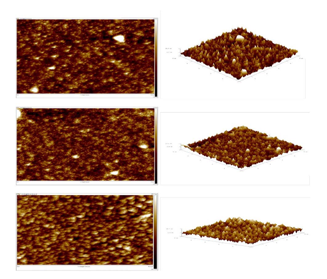
Figure 2: AFM DB1fA Annealed at 100, 150 & 200o C respectively top to bottom. Height 2D (left) & 3D (right).
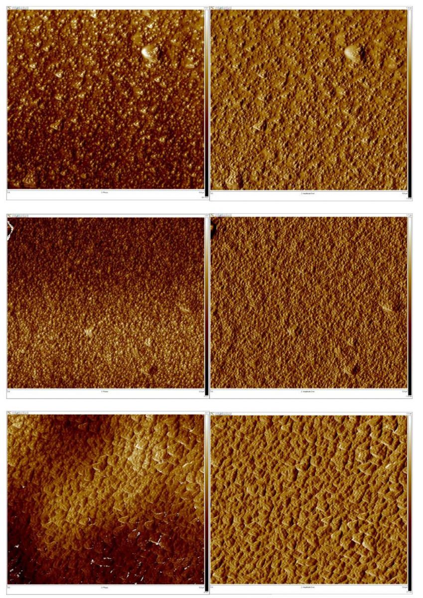
Figure 3: AFM DB1fA Annealed at 100, 150 & 200o C respectively top to bottom (left) Phase 2D and (right) Amplitude 2D.
Figure 4: Annealed temperature vs. surface roughness.
In this study, we observed that surface roughness or nanophase domain sizes playing a vital role for optoelectronic applications. If the surface roughness is too small (e.g., 4 nm), then the charge carrier pathways might be a problem due to small or not continuous domain grain sizes. Additionally, photon loss due to lack of reflection could be severe if surface are too smooth. On the other hand, if the domain sizes are too large, the D/A interface could be too small for efficient photo induced exciton dissociation. The intermediate roughness or domain size result in sizable donor/acceptor interface as well as continuous charge transport pathways and therefore exhibiting best optoelectronic performance. The optoelectronic properties appear correlated to the surface morphological roughness closely.
Solar cell device fabrications
A 1:1 ratio of DB1fA polymer and PC70BM acceptor solution was prepared by dissolving 15mg of block copolymer and 15 mg of acceptor polymer in a one milliliter of o-Dichlorobenzene (DCB). All of the devices with DB1fA block copolymer were prepared in a similar fashion. To ensure the polymer completely dissolved each was heated in a sand bath at 60-90oC overnight.
Delta-Tech 25x75x0.4mm ITO slides (5-100 Ohms resistance) were used; the ITO slide was examined using the Simpson electric multi-meter. ITO slide were cut out according to the shape on the pattern sheet typically two slides per ITO sheet. A piece of tape was placed on the middle of the glass slide to protect the ITO during etching, then the slides were placed in a 6M HCl for 10 minutes. The slides were removed and washed with deionized water and the tape was removed immediately to avoid sticky residue on slides. The ITO plates were sonicated for 5 minutes then washed in recycled 1) detergent; 2) DI water; 3) Acetone; 4) Isopropanol then air dried.
The PEDOT: PSS aqueous solution was spin coated on to the glass slide suing spin coater recipe #1 (5000rpm, 30s) yielding a 30-40nm thick PEDOT: PSS film. The films were placed in a vacuum oven for 90 minutes at 80oC to ensure the slides were dry. After the slide cooled to room temperature DB1fA and PCBM mixture solution were placed separately one several slides and spin coated on recipe #2 (1000rpm, 60s, 100- 300nm thickness). This spin coating recipe was optimized for P3HT to where this is not the optimum thickness for the materials being used. The device runs the risk that if the film is too thick there will be high resistance and if too low there will be low photon absorption. The films were placed in the vacuum oven at 80oC overnight.
The slides were removed from the vacuum oven and placed in the photovoltaic device fabrication glove box for aluminum deposition. Each slide contained 8 cells (Figure 5) to where each cell had a 1 cm by 1 cm area and a 128 nm thickness.
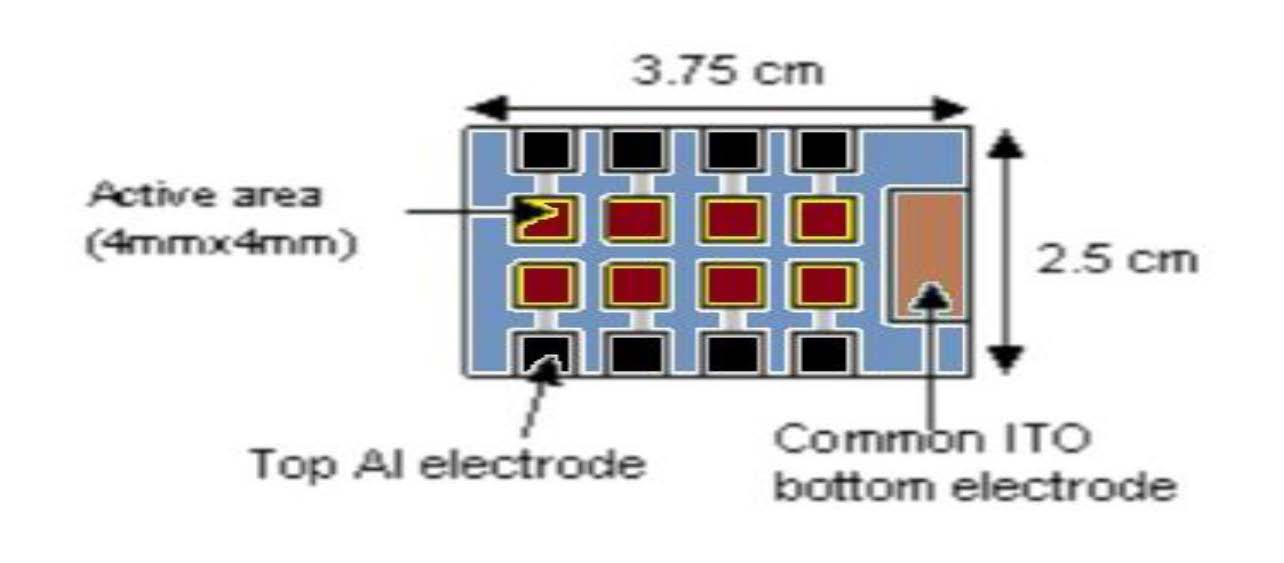
Figure 5: Scheme of eight solar cells fabricated on an ITO slide
Optoelectronic Device Studies
The solar cell device efficiency had been studied by AM 1.5G solar simulator with 80-100 mW/cm2 intensity. A Keithley 237 source-measure unit (SMU) was used to collect the voltage-current data that were processed by computer into J-V curves. A solar cell device had been built which is composed of multiple stack layers (ITO/PEDOT: PSS/Polymer: PC70BM/Al). Cells were made from and DB1fA as donor polymers and were fabricated into solar cell devices and compared. The short-circuit current density (Jsc), open-circuit voltage (Voc), fill factor (FF), and power conversion efficiencies (PCE) of fabricated cells are listed in Table 1. A best photo J-V curve (in log scale) among a set of eight cells made of either DB1fA are shown in Figure 6 for all the DB1fA ’s, where the intermediate surface roughness, the better the PCE. The absolute efficiencies of the cells reported here are relatively low compared to other literature reported best organic cell values (over 10%) due to, for instance, the PPVs reported here have much higher energy gaps (more than 2.2 eV) compared to popular donor type polymers (such as regio-regular P3HT) that exhibits lower energy gaps (less than 2.0 eV) and better charge transport, and our cell fabrication protocols as well as polymer solid state morphologies have not yet been systematically optimized. However, higher energy gaps and fluorination of the conjugated polymer may find important applications in certain higher energy radiations or in applications where hydrophobicity is desired [14].
Table 1: Solar Cell Performance of DB1fA’s
|
Thermal Annealing |
Voc (volt) |
Jsc (mA/cm2) |
FF% |
PCE% |
|
100oC |
0.77 |
0.24 |
37.01 |
0.137 |
|
150oC |
0.66 |
0.04 |
31.29 |
0.02 |
|
200oC |
0.49 |
0.01 |
23.14 |
0.000000085 |
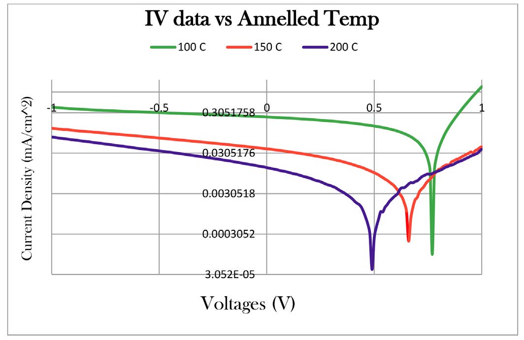
Figure 6: DBf1A’s IV data Comparisons.
CONCLUSIONS
Solid state morphologies of the conjugated block copolymer DB1fA were investigated via polymer films processing protocols including film thickness, thermal annealing temperature, cleaning of ITO glasses, etc. This study demonstrated that an intermediate surface roughness of about 8 nm yielded orders of magnitude better optoelectronic device performances as compared to surface roughness of either smaller 4 nm or larger 14 nm surface morphologies. This study reveals that conjugated block copolymer morphology is essential for its optoelectronic properties. Further systematic optimizations of donor and acceptor block frontier orbital levels and the solid-state morphologies may lead to even higher optoelectronic power conversion efficiencies.
ACKNOWLEDGEMENTS
This material is based upon work supported, in parts, by research and/or educational grant awards from a number of agencies including the US Department of Defense (Award # W911NF-15-1-0422) and the US National Science Foundation (NSF Award # HRD- 1547771).
REFERENCES
- Tang C (1986) Two- layer organic photovoltaic cell. Appl Phys Lett 48, 183.
- Sun S, Sariciftci N (2005) Organic Photovoltaics: Mechanisms, Materials and Devices [1st Ed.] CRC Press, Boca Raton, FL, USA.
- S Sun, HO’Neill (2011) Sunlight Energy Conversion via Organics, in Handbook of Photovoltaic Science and Engineering, [2nd Ed.] Wiley, the Atrium, England, p. 675-715.
- Y Li (2012) Molecular Design of Photovoltaic Materials for Polymer Solar Cells: Toward Suitable Electronic Energy Levels and Broad Absorption. Acc Chem Res 45(5): 723.
- TA Skotheim RL, Elsenbaumer (2007) J. R. Reynolds Handbook of Conducting Polymers. [3rd Ed.] CRC Press, Boca Raton, FL, USA.
- Hadjichristidis N, Pispas S, Floudas (2003) Block Copoly- mers: Synthetic Strategies, Physical Properties, and Applications. John Wiley & Sons, NY, USA.
- Hamley IW (1998) The Physics of Block Copolymers. Oxford University Press, Oxford, U.K.
- Bates FS, Fredrickson GH (1990) The Block Copolymer Thermodyanmics: Theory and experiment. Annu Rev Phys Chem 4: 525-557.
- Sun S, Dalton L (2016) Introduction to Organic Electronic and Optoelectronic Materials and Devices. [2nd Ed.] CRC Press/Taylor & Francis, Boca Raton, FL, USA.
- S. Sun(2003). Design of a Block Copolymer Solar Cell. Sol. Energy Mat. Sol. Cell 79(2):257-264
- Sun S (2016) Basic Electronic Structures and Charge Carrier Generation in Organic Optoelectronic Materials, in Introduction to Organic Electronic and Optoelectronic Materials and Devices. [2nd Ed.] CRC Press/Taylor & Francis, Boca Raton, FL, USA.
- Sun S, Brook J, Nguyen T, Zhang C (2014) “Design, Synthesis, and Characterization of a Novel c-Donor-nc-Bridge-c-Acceptor Type Block Copolymer For Optoelectronic Applications”. J Poly Sci Poly Chem 52(8): 1149-1160.
- Biju, Sudeep P, Thomas K, George M, Barazzouk S, Kamat P (2002) Clusters of Bis- and Tris-Fullerenes. Langmuir 18(5): 1831-1839.
- Nguyen T, Hasib M, Wang D, Sun S (2016) Design, Synthesis, Characterization, and Optoelectronic Properties of a Novel c-Donor-nc-Bridge-cf-Acceptor Type Block Copolymer. J Res Up Poly Sci 5: 18-38.
- Hasib, M, Sun S (2019) “Effects of Different Bridges of A Series of c-Donor-nc-Bridge-cf- Acceptor Type Block Copolymers for Potential Solar Cell Applications”. J Res Up Poly Sci 8: 27-34.
- Rohr T, van Eesbeek M (2005) In Proceeding of the 8th Polymers for Advanced Technologies International Symposium. Budapest, Hungary.
Copyright: Sun SS ©2019. This is an open-access article distributed under the terms of the Creative Commons Attribution License, which permits unrestricted use, distribution, and reproduction in any medium, provided the original author and source are credited.
Citation: Sun SS (2019). Correlations of Morphology and Optoelectronic Property of a DB1fA Type Block Co-Polymer. Material Sci 1(1): 1.